디논실 lab1-2 정리
- 3 mins실습 환경
Vivado
FPGA 보드: Arty A7-100T라는 제품을 사용한다. 35T와는 DPS 슬라이스 개수, 슬라이스 개수가 더 많다.
DSP slice=a digital signal processing logic element included on certain FPGA device familie
Verilog 기초
자료형
wire: wire 또는 always 구문 밖에서 값이 조작되는 변수
reg: register always 구문 내에서 값이 조작되는 변수는 반드시 reg형
always @(조건), begin, end
- always @*: always 구문 내 입력 변수 변화가 있으면 언제나 실행
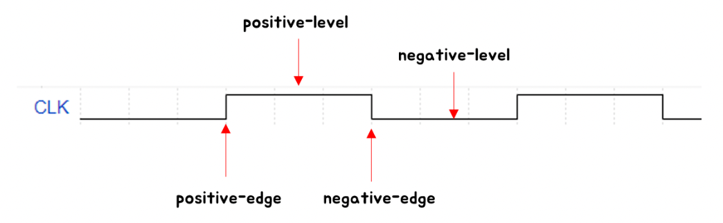
- always @ (posedge CLK) : CLK 신호가 positive edge 일 때 실행
- always @ (posedge CLK or negedge RESETn): CLK 신호가 postiive edge 일때 또는 RESETn 신호가 negative edge 일때 combinational logic 과 sequential logic의 차이는 출려값이 입력값에만 영향을 받는 회로가 comb. logic이고, sequential logic은 출력값이 입력값과 이전 입력들의 영향을 받는 회로이다.
할당연산자로는
- combinational logic 은 ‘=’
- seqeuntial lgoic 은 ‘<=’
숫자 표현은 4’b1111 => bit수’진수, 수 로 표현한다.
잉여 조건 정의되지 않은 조건이 존재하는 경우 Latch 가 발생한다. Latch란 저레벨의 직렬화 메커니즘이다. 메로리 기능을 가지고 있는 회로로 입력상태를 저장하고 저장한 상태를 유지한다.
Triger 종류
Test bench 작성방법
input, output을 비슷하게 선언해주고 모듈처럼 사용해서 입력을 넣어주면된다. 밑에는 initial, begin, end를 활용해 입력값을 넣어주면 된다. 이때 #은 ns만큼 wait한다.
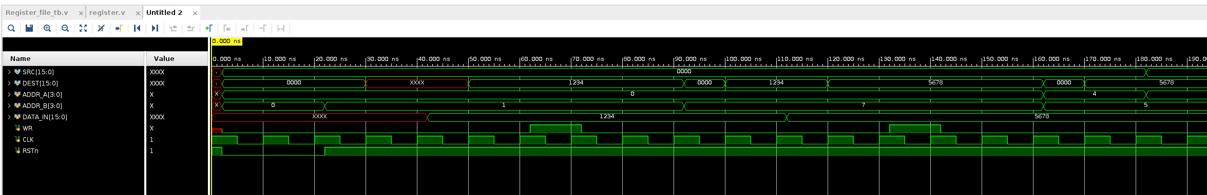
실험 결과 
Lab2 : Register File
Read operation의 경우 Addr_A, Addr_B를 읽어 Src, Dest에 출력하는 operation, CLK의 영향을 받지 않는 cominational logic
Write operation의 경우 Addr_B위치에 Data_in(ALU의 계산 결과)를 write한다. 조건은 CLK: rising edge, WR: positive 일때, CLK의 영향을 받는 sequential logic
module register(
    CLK, RSTn, ADDR_A, ADDR_B, DATA_IN, WR, SRC, DEST
    );
    output reg [15:0] SRC, DEST;

    input [3:0] ADDR_A, ADDR_B;
   input [15:0] DATA_IN;
    input WR, CLK, RSTn;

   reg [15:0] array [7:0];

always@*
begin
   SRC = array[ADDR_A];
   DEST = array[ADDR_B];
end

always@(posedge CLK or negedge RSTn)
begin
    if(!RSTn) begin
        array[0] <= 16'h0000;
        array[1] <= 16'h0000;
        array[2] <= 16'h0000;
        array[3] <= 16'h0000;
        array[4] <= 16'h0000;
        array[5] <= 16'h0000;
        array[6] <= 16'h0000;
        array[7] <= 16'h0000;
    end
    else begin
        array[ADDR_B] <= DATA_IN;
    end
end
endmodule